


1.Basic Concepts
Charge and Conductivity
In the Bohr theory of the atom (named after Niels Bohr, 1885—1962), electrons orbit a nucleus containing neutrons and protons. Attraction between the opposite charges of electrons and protons keeps atoms together. Particles with the same charge repel each other.
Electric charge is measured in coulombs (C). An individual electron or proton has much less than one coulomb of charge, -1.6×10 -19 C on an electron, 1.6×10 -19 C on a proton. Nature says only that an electron's charge is the opposite of a proton's; there is nothing inherently negative about electrons, they could just as easily be called negative and protons positive.
The electrons of different types of atoms have different degrees of freedom to move around. With some types of materials, such as metals, the outermost electrons in the atoms are so loosely bound that they chaotically move in the space between the atoms of that material by nothing more than the influence of room-temperature heat energy. Because these virtually unbound electrons are free to leave their respective atoms and float around in the space between adjacent atoms, they are often called free electrons.
In other types of materials such as glass, the atoms' electrons have very little freedom to move around. While external forces such as physical rubbing can force some of these electrons to leave their respective atoms and transfer to the atoms of another material, they do not move between atoms within that material very easily.
This relative mobility of electrons within a material is known as electric conductivity. Conductivity is determined by the types of atoms in a material (the number of protons in each atom's nucleus, determining its chemical identity) and how the atoms are linked together with one another. Materials with high electron mobility (many free electrons) are called conductors, while materials with low electron mobility (few or no free electrons) are called insulators.
It should also be understood that some materials experience changes in their electrical properties under different conditions. Glass, for instance, is a very good insulator at room temperature, but becomes a conductor when heated to a very high temperature. Gases such as air, normally insulating materials, also become conductive if heated to very high temperatures. Most metals become poorer conductors when heated, and better conductors when cooled. Many conductive materials become perfectly conductive (this is called superconductivity) at extremely low temperatures.
While the normal motion of “free” electrons in a conductor is random, with no particular direction or speed, electrons can be influenced to move in a coordinated fashion through a conductive material. This uniform motion of electrons is what we call electricity, or electric current. Just like water flowing through the emptiness of a pipe, electrons are able to move within the empty space within and between the atoms of a conductor. The conductor may appear to be solid to our eyes, but any material composed of atoms is mostly empty space! There can be electric current only where there exists a continuous path of conductive material providing a conduit for electrons to travel through. If the path is blocked, the “flow” will not occur.
Electric Circuits , Voltage and Current
An electric circuit is formed when a conductive path is created to allow free electrons to continuously move. This continuous movement of free electrons through the conductors of a circuit is called a current, and it is often referred to in terms of “flow”, just like the flow of a liquid through a hollow pipe.
The force motivating electrons to “flow” in a circuit is called voltage, which technically is a measure of potential energy per unit charge of electrons. The most familiar form of potential energy is gravitational potential energy. Because of the gravitational attraction between the earth and the objects on it, lifting objects gives them potential energy. The more mass something has and the higher we lift it, the more potential energy it has. When we speak of a certain amount of voltage being present in a circuit, we are referring to the measurement of how much potential energy exists to move electrons from one particular point in that circuit to another particular point. Without reference to two particular points, the term “voltage” has no meaning.
Voltage is usually indicated by the symbol V , measured in volts (symbol: V), named after Alessandro Volta (1745—1827). One volt is defined as that magnitude of electromotive force required causes a current of one ampere to pass through a conductor having a resistance of one ohm. In digital circuits, we sometimes measure voltage in thousands of a volt, or millivolts (mV). Increasing the voltage of one coulomb of charge by one volt gives it one joule (J) of electrical potential energy, named after James P. Joule (1818—1889). Because electrons have negative charge, we have to take electrons from a higher to a lower voltage to increase their potential energy.
Any source of voltage, including batteries, has two points for electrical contact. We can provide such a path for the battery by connecting a piece of wire from one end of the battery to the other. Forming a circuit with a loop of wire, we will initiate a continuous flow of electrons in a clockwise direction, as shown in Fig.2-1.
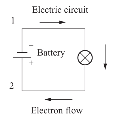
Fig.2-1 Current in a anti-clockwise direction
So long as the battery continues to produce voltage and the continuity of the electrical path isn't broken, electrons will continue to flow in the circuit. Following the metaphor of water moving through a pipe, this continuous, uniform flow of electrons through the circuit is called a current. So long as the voltage source keeps “pushing” in the same direction, the electron flow will continue to move in the same direction in the circuit. This single-direction flow of electrons is called Direct Current, or DC. When the direction of current switches back and forth, it is called Alternating Current, or AC.
Because electric current is composed of individual electrons flowing in unison through a conductor by moving along and pushing on the electrons ahead, just like marbles through a tube or water through a pipe, the amount of flow throughout a single circuit will be the same at any point. If we were to monitor a cross-section of the wire in a single circuit, counting the electrons flowing by, we would notice the exact same quantity per unit of time as in any other part of the circuit, regardless of conductor length or conductor diameter.
Current flow is represented by the letter symbol I . The basic unit in which current is measured is the ampere (A). One ampere of current is defined as the movement of one coulomb past any point of a conductor during one second of time. The other unit is milliampere (mA) or microampere (μA).
Resistance , Capacitance and Inductance
Free electrons tend to move through conductors with some degree of friction, or opposition to motion. This opposition to motion is more properly called resistance. The amount of current in a circuit depends on the amount of voltage available to motivate the electrons, and also the amount of resistance in the circuit to oppose electron flow. Just like voltage, resistance is a quantity relative between two points. For this reason, the quantities of voltage and resistance are often stated as being “between” or “across” two points in a circuit.
The device to be capable of doing this is called a resistor. The amount of resistance to the flow of current that a resistor causes depends on the material it is made of as well as its size and shape. Some resistors obey Ohm's law, which states that the current density is directly proportional to the electrical field when the temperature is constant.
The resistance of a material that follows Ohm's law is constant, or independent of voltage or current, and the relationship between current and voltage is linear. Modern electronic circuits depend on many devices that deviate from Ohm's law. In devices such as diodes, the current does not increase linearly with voltage and is different for two directions of current. Resistors are often made to have a specific value of resistance so that the characteristics of the circuit can be accurately calculated.
Electrical resistance is represented by the letter symbol R . The unit of resistance is the ohm, a term that is often expressed by using Ω. One ohm is defined as that amount of resistance that will limit the current in a conductor is one ampere when the voltage applied to the conductor is one volt. Larger amounts of resistance are commonly expressed in kiloohm (kΩ) or in megohm (MΩ).
Whenever an electric voltage exists between two separated conductors, an electric field is present within the space between those conductors. Electrical energy can be stored in an electric field. The device to be capable of doing this is called a capacitor or a condenser. Capacitors are components de signed by placing two conductive plates (usually metal) in close proximity with each other. A capacitor's ability to store energy as a function of voltage (potential difference between the two leads) results in a tendency to try to maintain voltage at a constant level. In other words, capacitors tend to resist changes in voltage drop. When voltage across a capacitor is increased or decreased, the capacitor “resists” the change by drawing current from or supplying current to the source of the voltage change, in opposition to the change.
If a condenser is connected to a battery, the electrons will flow out of the negative terminal of the battery and accumulate on the condenser plate connected to that side. Thus the condenser is said to be charged. The capacitance is directly proportional to the dielectric constant of the material and to the area of the plates and inversely to the distance of the plates. The larger the plate area, the smaller the space between them, the greater the capacitance.
The measure of a capacitor's ability to store energy for a given amount of voltage drop is called capacitance. Not surprisingly, capacitance is also a measure of the intensity of opposition to changes in voltage (exactly how much current it will produce for a given rate of change in voltage). Capacitance is symbolically denoted with a capital C , and is measured in the unit of the Farad, abbreviated as F. When farad is a too large unit to be used in radio calculation, so microfarad and picofarad are used.
Whenever electrons flow through a conductor, a magnetic field will develop around that conductor. This effect is called electromagnetism. Magnetic energy can be stored in a magnetic field. The device to be capable of doing this is called an inductor. An inductor is simply a coil of wire with or without a magnetic core. Energy storage in an inductor is a function of the amount of current through it. An inductor's ability to store energy as a function of current results in a tendency to try to maintain current at a constant level. In other words, inductors tend to resist changes in current. When current through an inductor is increased or decreased, the inductor “resists” the change by producing a voltage between its leads in opposing polarity to the change.
To store more energy in an inductor, the current through it must be increased. This means that its magnetic field must increase in strength, and that change in field strength produces the corresponding voltage according to the principle of electromagnetic self-induction. When the current through an inductor is increased, it drops a voltage opposing the direction of electron flow, acting as a power load. In this condition the inductor is said to be charging, because there is an increasing amount of energy being stored in its magnetic field. Note the polarity of the voltage with regard to the direction of current.
The measure of an inductor's ability to store energy for a given amount of current flow is called inductance. Not surprisingly, inductance is also a measure of the intensity of opposition to changes in current (exactly how much self-induced voltage will be produced for a given rate of change of current). Inductance is symbolically denoted with a capital L and is measured in the unit of the Henry, abbreviated as H.
2.Circuit and System
Ohm's Law
As stated before, voltage is the measure of potential energy per unit charge available to motivate electrons from one point to another, current is the rate of electric charge motion through a conductor, resistance is the opposition for free electrons to motion through conductors. These units and symbols for electrical quantities will become very important to know as we begin to explore the relationships between them in circuits. The first, and perhaps most important, relationship between current, voltage, and resistance is called Ohm's Law, discovered by Georg Simon Ohm in 1827. Ohm's principal discovery was that the amount of electric current through a metal conductor is directly proportional to the voltage impressed across it, for any given temperature.
Ohm's Law is given by

where V is the potential difference between two points which include a resistance R , I is the current flowing through the resistance. When the conductance, g =1 /R , is used, Ohm's Law in this form is

If we know the values of any two of the three quantities (voltage, current and resistance) in a cir-cuit, we can use Ohm's Law to determine the third.
Kirchoff's Current Law and Kirchoff's Voltage Law
There are more complicated circuits which cannot be reduced to simply a parallel or series circuit using equivalent resistances. Instead, these need to be solved using two concepts: Kirchhoff's Current Law and Kirchhoff's Voltage Law.
In Fig.2-2, we see that I 1 is the only current flowing into the node. However, there are three paths for current to leave the node, and these current are represented by I 2 , I 3 , and I 4 .
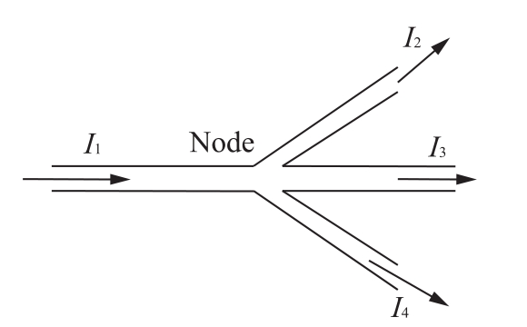
Fig.2-2 Current flowing into and out of a node
Once charge has entered into the node, it has no place to go except to leave (this is known as conservation of charge). The total charge flowing into a node must be the same as the total charge flowing out of the node. So,

Bringing everything to the left side of the above equation, we get

Then, the sum of all the currents is zero. This can be generalized as

Note the convention we have chosen here: current flowing into the node is taken to be negative, and currents flowing out of the node are positive.
Kirchhoff's Voltage Law (or Kirchhoff's Loop Rule) is a result of the electrostatic field being conservative. It states that the total voltage around a closed loop must be zero. If this were not the case, then when we travel around a closed loop, the voltages would be indefinite. So,

Introduction to Network Theorems
In electric network analysis, the fundamental rules are Ohm's Law and Kirchhoff's Laws. While these humble laws may be applied to analyze just about any circuit configuration (even if we have to resort to complex algebra to handle multiple unknowns), there are some “shortcut” methods of analysis to make the math easier.
Superposition Theorem
The strategy used in the Superposition Theorem is to eliminate all but one source of power within a network at a time, using series/parallel analysis to determine voltage drops (and/or currents) within the modified network for each power source separately. Then, once voltage drops and/or currents have been determined for each power source working separately, the values are all “superimposed” on top of each other (added algebraically) to find the actual voltage drops/currents with all sources active.
Thevenin's Theorem
Thevenin's Theorem states that it is possible to simplify any linear circuit, no matter how complex, to an equivalent circuit with just a single voltage source and series resistance connected to a load. The qualification of “linear” is identical to that found in the Superposition Theorem, where all the underlying equations must be linear (no exponents or roots). If we're dealing with passive components (such as resistors, inductors and capacitors), this is true. However, there are some components (especially certain gas-discharge and semiconductor components) which are nonlinear: that is, their opposition to current changes with voltage and/or current. As such, we would call circuits containing these types of components, nonlinear circuits.
Thevenin's Theorem is especially useful in analyzing power systems and other circuits where one particular resistor in the circuit (called the “load” resistor) is subject to change, and re-calculation of the circuit is necessary with each trial value of load resistance, to determine voltage across it and current through it.
Steps to follow for Thevenin's Theorem:
1)Find the Thevenin source voltage by removing the load resistor from the original circuit and calculating voltage across the open connection points where the load resistor used to be.
2) Find the Thevenin resistance by removing all power sources in the original circuit (voltage sources shorted and current sources open) and calculating total resistance between the open connection points.
3)Draw the Thevenin equivalent circuit, with the Thevenin voltage source in series with the Thevenin resistance. The load resistor re-attaches between the two open points of the equivalent circuit.
4)Analyze voltage and current for the load resistor following the rules for series circuits.
Norton's Theorem
Norton's Theorem states that it is possible to simplify any linear circuit, no matter how complex, to an equivalent circuit with just a single current source and parallel resistance connected to a load. Just as with Thevenin's Theorem, the qualification of “linear” is identical to that found in the Superposition Theorem: all underlying equations must be linear (no exponents or roots).
Steps to follow for Norton's Theorem:
1) Find the Norton source current by removing the load resistor from the original circuit and calculating current through a short (wire) jumping across the open connection points where the load resistor used to be.
2) Find the Norton resistance by removing all power sources in the original circuit (voltage sources shorted and current sources open) and calculating total resistance between the open connection points.
3)Draw the Norton equivalent circuit, with the Norton current source in parallel with the Norton resistance. The load resistor re-attaches between the two open points of the equivalent circuit.
4)Analyze voltage and current for the load resistor following the rules for parallel circuits.
NEW WORDS AND PHRASES
charge n . 负荷,电荷,费用,主管,掌管,充电,充气
conductivity n . 传导性,传导率
insulator n . 绝缘体,绝热器
gravitational adj . 重力的
voltage n . [电]电压,伏特数
volts n . 直流电压
ampere n . 安培
ohm n . [物]欧姆
coulomb n . [电]库仑(电量单位)
diameter n . 直径
inductance n . 感应系数,自感应
condenser n . 冷凝器,电容器
dielectric n . 电介质,绝缘体; adj .非传导性的
farad n . [电]法拉(电容单位)
picofarad n . [电]皮(可)法拉,微微法拉,百亿分之一法拉
magnetic core 磁心
polarity n . 极性
potential difference [电]电位差,电势差
equivalent resistance 等效电阻
Superposition Theorem 叠加定理
Thevenin's Theorem 戴维南定理
Norton's Theorem 诺顿定理
NOTES
1) So long as the battery continues to produce voltage and the continuity of the electrical path isn't broken, electrons will continue to flow in the circuit.
只要电池持续供电,并且导线没有断开,电子将始终在回路中流动。
2) If a condenser is connected to a battery, the electrons will flow out of the negative terminal of the battery and accumulate on the condenser plate connected to that side. Thus the condenser is said to be charged.
当电容与电池相连,电子将从电池的负极流出,并聚集在电容与该端相连的极板上,称电容充电。
3)Whenever electrons flow through a conductor, a magnetic field will develop around that conductor.
只要电子束流过导体,就将在这个导体周围产生磁场。
4) Glass, for instance, is a very good insulator at room temperature, but becomes a conductor when heated to a very high temperature.
例如,玻璃在室温下是一种非常好的绝缘体,但当把它加热到相当高的温度时它就变成一种导体。
5)Whenever an electric voltage exists between two separated conductors, an electric field is present within the space between those conductors.
只要在两个独立的导体间存在电压,它们之间就会产生电场。
6)While the normal motion of “free” electrons in a conductor is random, with no particular direction or speed, electrons can be influenced to move in a coordinated fashion through a conductive material.
通常导体里的自由电子是随机运动的,没有确定的方向或速度,但是电子受力后可沿相同的方向通过导体。
EXERCISES
1.Please translate the following words and phrases into Chinese.
a)ampere
b)conductivity
c)magnetic core
d)insulator
e)dielectric
f)Thevenin's Theorem
g)negative terminal
h)charge
i)inductance
j)polarity
2.Please translate the following words and phrases into English.
a)电荷
b)电感
c)极性
d)节点
e)电阻器
f)电容器
g)绝缘体
h)等效电阻
i)叠加定理
j)电流
3.Fill in the blanks with the missing word(s).
a)Electric charge is measured in__________. An individual electron or proton has much less than one cou-lomb of charge, -1.6×10 -19 coulomb on an__________, 1.6 × 10 -19 on a__________.
b)Whenever electrons flow through a conductor, a__________field will develop around that conductor. This effect is called__________.
c)Magnetic energy can be stored in a magnetic field. The device to be capable of doing this is called an__________.
d)An inductor is simply a coil of wire with or without a magnetic core. Energy storage in an inductor is a function of the amount of__________through it.
e)When current through an inductor is__________or__________, the inductor“resists”the change by produ-cing a__________between its leads in opposing__________to the change.
f)Once charge has entered into the__________, it has no place to go except to leave.
g)Kirchhoff 's Voltage Law states that the total voltage around a closed loop must be__________.
4.Answer the following questions according to the text.
a)How the capacitors store energy?
b)What are the relationship between the voltage and the current?
c)What is the Ohm's Law?
d)What are the Kirchhoff's Current Law and Kirchhoff's Voltage Law?
e)What are the Thevenin's Theorem and Norton's Theorem?
半导体器件
Semiconductors are materials which are neither conductors or insulators, having conductivities intermediate to those of conductors like copper and insulators like wood or plastic. Common semiconductors are Silicon and Germanium. Semiconductor devices such as diodes, transistors and integrated circuits made possible miniaturized electronics, including computers, certain types of medical diagnostic and treatment equipment, and popular telecommunication devices, to name a few applications of this technology. We have come to rely on them and increasingly have come to expect higher performance at lower cost. Behind this revolution in technology stands an even greater revolution in general science: the field of quantum physics. Without this leap in understanding the natural world, the development of semiconductor devices (and more advanced electronic devices still under development) would never have been possible.
半导体是区别于导体和绝缘体的一种材料,其电导率介于铜这样的导体和木头、塑料这样的绝缘体之间。常见的半导体是硅和锗。半导体器件(如二极管、晶体管和集成电路)使得电子设备小型化成为可能,包括计算机、某类医疗诊断和治疗设备、通用的电信设备,这只是这项技术的很少的一些应用。我们越来越依赖这项技术,期望以更低的成本获得更高的性能。这项技术革命依赖于科学领域的更大的革命:量子物理学领域。没有这种对自然界的理解的飞跃,半导体器件的发展(和仍在开发中的更先进的电子设备)是不可能的。
1.Diode
1.二极管
Diode, electronic device that allows the passage of current in only one direction, has a low resistance to electric current in one direction and a high resistance to it in the reverse direction. When current flows from the P-type to the N-type material, the positive holes and the negative electrons are forced into close contact at the boundary. At the boundary, the electrons fill the holes across the boundary while the terminals supply new holes and electrons. Thus, in the forward bias case a continual current flows. In the reverse bias case, the charge carriers are pulled apart. There is no longer an easy way for electrons to tunnel through the barrier as there are no longer many empty holes waiting on the opposite side.
二极管是一种只允许单向电流通过的电子设备,对一个方向上的电流电阻低,对相反方向上的电流电阻高。当电流从P型材料到N型材料时,正的空穴和负的电子在边界相遇。在边界上,电子跨越边界填充空穴,产生新的空穴和电子。因此,在正向偏置情况下产生持续电流。在反向偏置情况下,电荷载流子被分开。电子不能穿过屏障,另一侧也不再有空穴。
The vacuum-tube diodes consist of an evacuated glass or steel envelope containing two electrodes: a cathode and an anode. Because electrons can flow in only one direction, from cathode to anode, the vacuum-tube diode could be used as a rectifier, which can convert Alternating Current(AC)into Direct Current(DC). Fig.2-3 demonstrates a simple half-wave rectifier.
真空二极管由抽空的玻璃管或金属壳构成,包含两个电极:一个是阴极,一个是阳极。因为电子只能从阴极到阳极单方向流动,所以真空管可用作整流器,将交流电(AC)变成直流电(DC)。图2-3所示为简单的半波整流器。
Since the current only flows one way through the resistor the voltage drop can never be negative. The capacitor serves merely as an extra voltage source to even out the sine wave. Fig.2-4 demonstrates the resulting voltage V s .
由于电流流过电阻的电压降不能为负,因此电容器只能作为额外的电压源使正弦波全部为正。图2-4给出了最终产生的电压 V s 的波形。
The term half-wave refers to the fact that in the absence of the capacitor, a voltage exists only during the time when the primary source is positive. One can make a steadier source with a full-wave rectifier as shown in Fig.2-5.
半波这个词是指如果没有电容器,只有当电源为正时才有电压存在。图2-5所示为带全波整流器的稳压源。
For the full-wave rectifier the current flows from left to right through the resistor for all parts of the AC cycle. This results in a positive voltage at all time as shown in Fig.2-6. The addition of capacitors would smooth out the resulting DC current even further.
在整个交流周期,全波整流器的电流从左到右通过电阻。在整个周期内电压均为正,如图2-6所示。加上电容器会使产生的直流电流更平滑。
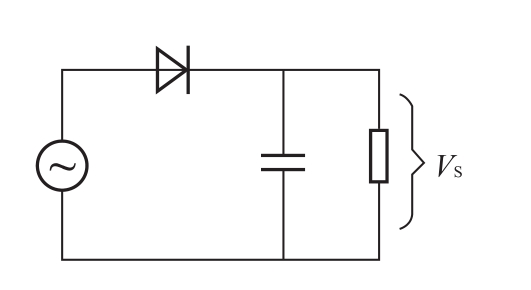
Fig.2-3 A simple half-wave rectifier
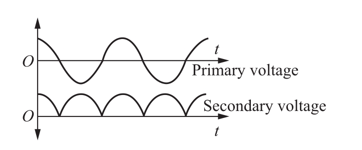
Fig.2-4 The capacitor serves even out the sine wave
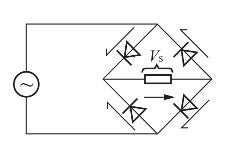
Fig.2-5 A full-wave rectifier
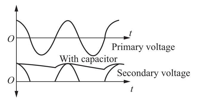
Fig.2-6 The capacitors smooth out the resulting DC current
When the voltage applied in the reverse direction exceeds a certain value, a semiconductor diode breaks down and conducts heavily in the direction of normally high resistance. When the reverse voltage at which breakdown occurs remains nearly constant for a wide range of currents, the phenomenon is called avalanching. A diode using this property is called a Zener diode. It can be used to regulate the voltage in a circuit.
当加在相反方向上的电压超过一定值时,半导体二极管击穿,在该方向导通且呈现高阻值。当电流在一定范围内变化时,反向击穿电压基本保持不变,这种现象称为雪崩。有这种属性的二极管称为齐纳二极管。它可以用来调节电路中的电压。
Semiconductor diodes can be designed to have a variety of characteristics.
半导体二极管具有多种特征。
One such diode, called a varactor, exhibits a capacitance that is dependent upon the voltage across it.
一种是变容二极管,其电容值依赖于两侧的电压。
In another kind, the tunnel diode, the current through the device decreases as the voltage is increased within a certain range; this property, known as negative resistance, makes it useful as an amplifier.
另一种是隧道二极管,当电压在一定范围内增加时,流经它的电流减少;这种特点称为负阻,使其可作为放大器。
Gunn diodes are negative-resistance diodes that are the basis of some microwave oscillators. Light-sensitive or photosensitive diodes can be used to measure illumination; the voltage drop across them depends on the amount of light that strikes them.
耿氏二极管是具有负阻效应的二极管,是微波振荡器的基本器件。光电二极管可以用来测量光照;它们的电压降取决于穿过它的光照量。
A Light-Emitting Diode(LED)produces light as current passes through it; some LEDs can act as the light source of lasers.
当电流通过发光二极管(LED)时会发光;一些LED可以作为激光光源。
However, some other forms of diode are created by depositing one material onto another, e.g. Schottky diodes are made by placing some metal in contact with a semiconductor. In general, whenever we join two different, very pure, materials we're likely to make some sort of diode.
然而,有些二极管通过把一种材料叠加在另一种材料上形成,如肖特基二极管把一些金属叠加在半导体上。通常,当加入两种不同的、纯的材料时,我们就可能会做出某些二极管。
Diodes are referred to as non-linear circuit elements. Fig.2-7 shows a schematic symbol for a diode and the current-voltage curve for an ideal diode.
二极管称为非线性电路器件。图2-7为理想二极管的原理符号和电流-电压曲线。
Diode is unidirectional, i.e. current flows in only one direction (anode to cathode internally). When a forward voltage is applied, the diode conducts; and when a reverse voltage is applied, there is no conduction.
二极管是单向的,即电流只能沿一个方向(阳极到阴极的内部)流动。当加正向电压时,二极管导通;当加反向电压时,二极管不导通。
Note that the diode conducts a small current in the forward direction up to a threshold voltage, 0.3V for germanium and 0.7V for silicon.
请注意,当电压达到阈值电压时,二极管导通,在正方向产生小电流,锗二极管的阈值电压为0.3V,硅二极管的阈值电压为0.7V。
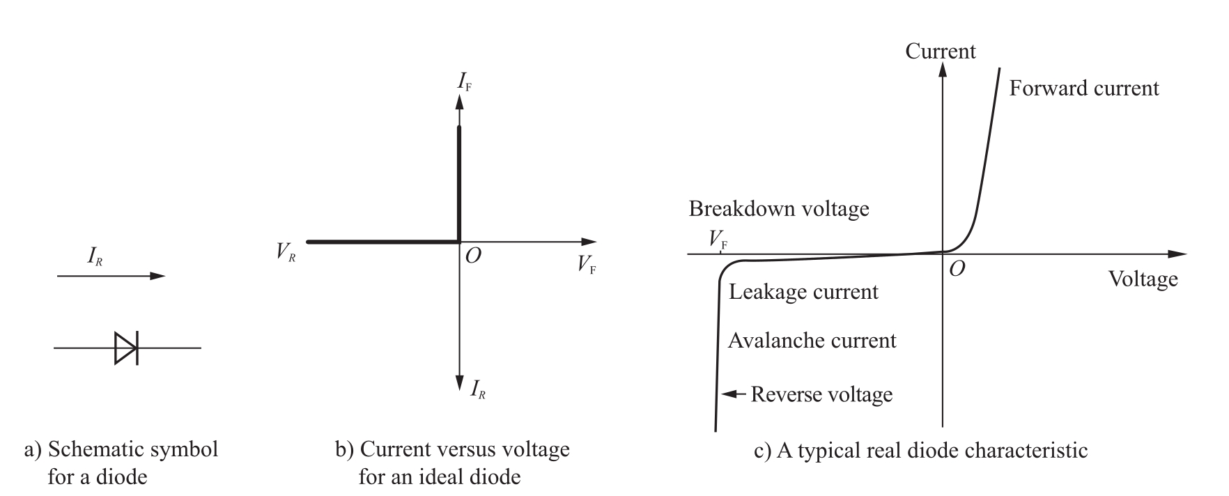
Fig.2-7 Diode
2.Transistors
2.晶体管
A transistor (see Fig.2-8) is the most crucial element in modern electronics. It serves as an amplifier and as a switch. A single transistor will adjust the output according to a small change in the input. Just as light switch can supply many hundreds of watts power by the flick of a finger. Before transistors, amplification and switching were done with vacuum tubes which are enormously bulky and produce a great deal of heat. Since a single microprocessor may hold near 5 million transistors, the advantage to 5 million vacuum tubes is obvious.
晶体管(见图2-8)是现代电子技术中最重要的器件。它可用作放大器和开关。晶体管将根据输入的微小变化调整输出。就像手指轻轻一按灯的开关就可以提供几百瓦功率。在晶体管出现之前,人们用真空管实现放大和开关,这不仅非常笨重而且会产生大量的热量。因为微处理器可包含近5百万个晶体管,所以其优势是显而易见的。
A transistor is constructed by sandwiching a layer of N-type semiconductor between two segments of P-type material.
晶体管在两层P型材料之间夹了一层N型半导体。
The small battery on the left serves as the switch. Without that portion of the circuit, the large battery can not pump current due to the N-P reverse bias of the right-hand loop. By adding a small voltage V E , a current flows through the left-hand loop which floods the narrow N-type region with charge which then destroys the ability of the N-P junction to stop the current. Thus a small voltage change in V E creates a large effect. Thus it can serve as either a switch or an amplifier. The circuit diagram for the transistor is shown on the left of Fig. 2-9. The upper left lead represents the emitter, the upper right lead represents the collector and the lower lead is the base.
左边的小电池作为开关。没有那部分电路,大电池不能产生右侧回路中的穿过N-P反向偏置的电流。加上较低的电压 V E 后,左侧回路中产生电流,该电流流过窄的N型区,破坏了N-P结对电流的阻止能力。因此,电压 V E 发生小的变化都要产生很大的影响。它可以作为开关或放大器。晶体管电路图显示在图2-9的左边。左上引线表示发射极,右上引线表示集电极,下引线表示基极。
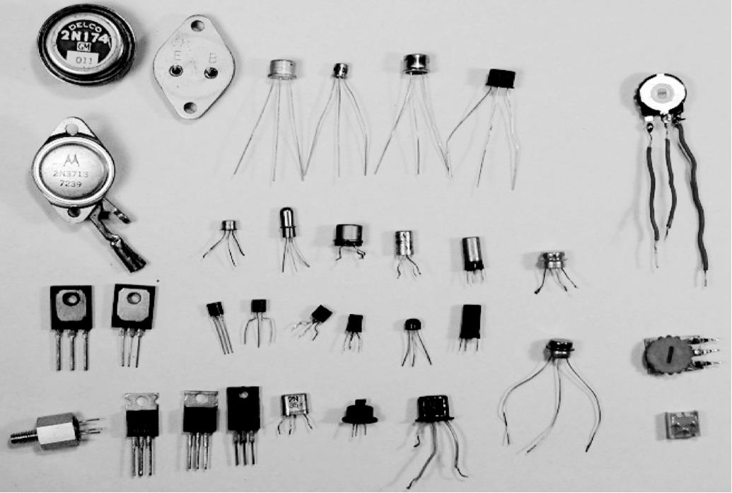
Fig.2-8 Some kinds of transistors
Bipolar Junction Transistors
双极结型晶体管
A bipolar transistor consists of a three-layer “sandwich” of doped (extrinsic) semiconductor materials, either PNP or NPN (see Fig.2-10). Each layer forming the transistor has a specific name, and each layer is provided with a wire contact for connection to a circuit. Shown here are schematic symbol and characteristic curve of NPN transistor types.
双极结型晶体管是一个由掺杂的半导体材料组成的三层的“三明治”(外形),或者PNP或者NPN(见图2-10)。形成晶体管的每一层都有特定的名称,每一层都设有用于连接到电路的导线。这里给出的是NPN型晶体管的原理符号与特性曲线。
We all know, in theory, the PNP characteristic curves look like the common NPN curves just by rotating the PNP plot by 180°. In swapping N for P so NPN→PNP, we've reversed the direction of current flows (so currents are negative—flowing out of the collector and base in a PNP) and the required supply voltage becomes negative for a PNP.For any given state of operation, the current directions and voltage polarities for each type of transistor are exactly opposite to each other. Bipolar transistors work as current-controlled current regulators. In other words, they restrict the amount of current that can go through them according to a smaller, controlling current. The main current that is controlled goes from collector to emitter, or from emitter to collector, depending on the type of transistor it is (PNP or NPN, respectively). The small current that controls the main current goes from base to emitter, or from emitter to base, once again depending on the type of transistor it is (PNP or NPN, respectively). According to the confusing standards of semiconductor symbology, the arrow always points against the direction of electron flow, bipolar transistors are called bipolar because the main flow of electrons through them takes place in two types of semiconductor material:P and N, as the main current goes from emitter to collector (or vice versa). In other words, two types of charge carriers (electrons and holes) comprise this main current through the transistor.
我们都知道,在理论上,将PNP特性曲线旋转180°,PNP的特性曲线与NPN的特性曲线看起来一样。交换N和P,NPN就变成了PNP,我们把电流流向反向(所以电流是负的——在PNP中从集电极和基极流出),并且PNP所需的电源电压为负。对于任何给定的工作状态,每种类型的晶体管的电流方向与电压极性完全相反。双极晶体管是电流控制的电流调节器。换句话说,要限制晶体管中电流的大小,使其工作在小的控制电流下。受控的主电流是从集电极到发射极,或者从发射极到集电极,这取决于它的晶体管类型(分别是PNP型或NPN型)。控制主电流的小电流是从基极到发射极,或者从发射极到基极,同样取决于它的晶体管类型(分别是PNP型或NPN型)。根据半导体符号学的标准符号,箭头常常指向电子流动的方向,双极晶体管之所以是双极的,是因为流经的主电流主要发生在两种类型的半导体材料中:P和N,如从发射极到集电极(反之亦然)。换句话说,两种类型的电荷载流子(电子和空穴)构成主电流通过晶体管。
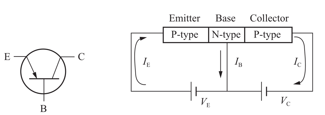
Fig.2-9 Schematic symbol for a transistor and construct a transistor by sandwiching
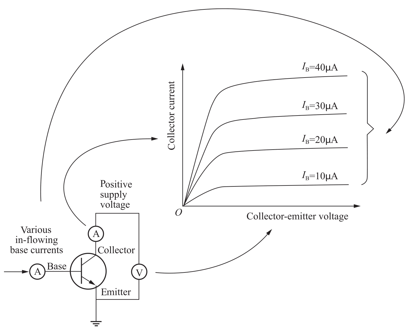
Fig.2-10 Symbol and characteristic curve of NPN transistor types
As you can see, the controlling current and the controlled current always mesh together through the emitter wire, and their electrons always flow against the direction of the transistor's arrow. This is the first and foremost rule in the use of transistors: all currents must be going in the proper directions for the device to work as a current regulator. The small, controlling current is usually referred to simply as the base current because it is the only current that goes through the base wire of the transistor. Conversely, the large, controlled current is referred to as the collector current because it is the only current that goes through the collector wire. The emitter current is the sum of the base and collector currents, in compliance with Kirchhoff's Current Law. If there is no current through the base of the transistor, it shuts off like an open switch and prevents current through the collector. If there is a base current, then the transistor turns on like a closed switch and allows a proportional amount of current through the collector. Collector current is primarily limited by the base current, regardless of the amount of voltage available to push it.
可以发现,控制的电流和受控的电流总是交织在一起流过发射极的导线,其电子流过的方向总是与晶体管的箭头方向相反。这是使用晶体管的首要规则:所有电流必须要在正确的方向以保证器件用作电流调节器。小的控制电流通常简称为基极电流,因为它是唯一流经晶体管基极导线的电流。相反,大的受控电流称为集电极电流,因为它是唯一流经晶体管集电极导线的电流。发射极电流是基极和集电极电流的总和,遵从基尔霍夫电流定律。如果没有电流流过晶体管的基极,它就像一个打开的开关,防止电流流过集电极。如果有基极电流,晶体管就像一个闭合的开关,允许成正比的电流量流过集电极。集电极电流主要由基极电流控制,忽略加在其上的电压。
Junction Field-Effect Transistors
结型场效应晶体管
In switching applications, Field Effect Transistors(FET)are preferred because they consume less power. FETs also have a NPN(or PNP)sequence of materials. However, the conductivity is controlled through the so-called gate that is electrically insulated from the device itself. By adjusting the voltage between the gate and the substrate, the width of a conducting channel between source and drain can be controlled. A FET is a unipolar device, conducting a current using only one kind of charge carrier. If based on an N-type slab of semiconductor, the carriers are electrons. Conversely, a P-type based device uses only holes. Functionally, the following correspondences between BJT and FET exist: base-gate, source-collector, drain-emitter.
当作为开关使用时,场效应晶体管(FET)因为功耗较小而成为首选。场效应晶体管也有NPN(或PNP)材料。然而,其导通性通过所谓的栅极控制,栅极与器件是电绝缘的。通过调整栅极和衬底之间的电压,可以控制源极和漏极之间沟道的宽度。场效应晶体管是一种单极型器件,只使用一种电荷载流子。如果场效应晶体管基于N型半导体,则载流子是电子。相反,如果场效应晶体管基于P型半导体,则载流子是空穴。从功能上讲,BJT和FET之间的对偶关系为:基极对应栅极,源极对应集电极,漏极对应发射极。At the circuit level, FET operation is simple. A voltage applied to the gate, input element, controls the resistance of the channel, the unipolar region between the gate regions. In an N-channel device, this is a lightly doped N-type slab of silicon with terminals at the ends. The source and drain terminals are analogous to the emitter and collector, respectively, of a BJT. In an N-channel device, a heavy P-type region on both sides of the center of the slab serves as a control electrode, the gate. The gate is analogous to the emitter of a BJT. The unipolar FET is conceptually simple, but difficult to manufacture. Most transistors today are a metal-oxide-semiconductor variety of the FET contained within integrated circuits. However, discrete JFET devices are available.
就电路性能而言,FET操作简单。在输入单元栅极加上电压,控制沟道的电阻。N沟道场效应晶体管是在两极的硅中掺杂少量N型杂质。源极和漏极分别类似于BJT的发射极与集电极。N沟道场效应晶体管在中心介质的两侧高参杂P型区作为控制电极——栅极。栅极类似于BJT的发射极。单极型场效应晶体管的概念很简单,但很难制造。现在集成电路中的晶体管,大多数是金属-氧化物-半导体场效应管。然而,也有分立的JFET。
Metal-Oxide-Semiconductor Field-Effect Transistors(MOSFET)
金属-氧化物-半导体场效应晶体管(MOSFET)
The most common FET technology is called MOSFET for Metal-Oxide-Semiconductor FET. P-type and N-type MOSFETs are combined to form CMOS(Complementary MOS)logic gates. Today, most transistors are of the MOSFET type as components of digital integrated circuits.
最常见的FET是金属-氧化物-半导体场效应晶体管(MOSFET)。P型和N型MOSFET组合形成CMOS(互补金属-氧化物-半导体)逻辑门。现在,大多数MOSFET型晶体管是数字集成电路中的基本器件。
A conceptually similar structure was proposed and patented independently by Lilienfeld and Heil in 1930, but the MOSFET was not successfully demonstrated until 1960. The main technological problem was the control and reduction of the surface states at the oxide-semiconductor interface. A reduction of the surface states enabled the fabrication of devices, which do not have a conducting channel unless a positive voltage is applied. Such devices are referred to as “enhancement-mode” devices. The electrons at the oxide-semiconductor interface are concentrated in a thin(~10nm thick)“inversion” layer. By now, most MOSFETs are “enhancement-mode” devices.
1930年Lilienfeld和Heil分别提出了一个概念相似的结构并申请了专利,但直到1960才成功地制成了MOSFET。主要技术问题是在氧化物-半导体界面控制和减少表面态。表面态的减少,使器件的制造成为可能,当加上正电压时才能形成导电沟道。这种器件称为“增强型”的。在氧化物-半导体界面上的电子集中在一个薄的(约10nm厚)“反转”层。现在,大多数的MOSFET是“增强型”的。
The MOSFET transistor count within an integrated circuit may approach the hundreds of a million. Much larger MOSFETs are capable of switching nearly 100A of current at low voltages; some handle nearly 1000V at lower currents. MOSFETs find much wider application than FETs. However, MOSFET power devices are not as widely used as bipolar junction transistors at this time.
集成电路中的MOSFET晶体管的数目可以多达几百万、几千万。更大的MOSFET能够在较低电压达到近100A的电流;有一些在较低的电流可得到近1000V的电压。MOSFET的应用比FET更广泛。然而,现在MOSFET功率器件不如双极结型晶体管应用广泛。
The voltage gain of the MOSFET is caused by the current saturation at higher drain-source voltages, so that a small drain current variation can cause a large drain voltage variation.
MOSFET中较高的漏-源电压引起电流饱和,从而产生电压增益,因此,小的漏极电流的变化可以引起大的漏极电压的变化。
The behavior of an enhancement N-channel MOSFET (NMOSFET) is largely controlled by the voltage at the gate (usually a positive voltage). For the usual drain-source voltage drops (i.e., the saturation region: positive voltages from a few volts up to some breakdown voltage), the drain current ( I D ) is nearly independent of the drain-source voltage ( V DS ), and instead depends on the gate voltage ( V G ). (This is unusual behavior: usually more voltage produces to more current, but here the current only increases slightly with increasing V DS .)
增强型N沟道MOSFET(NMOSFET)的行为主要由栅极的电压控制(通常是正电压)。对于通常的漏-源电压降(即饱和区:从几伏到击穿电压的正电压),漏极电流( I D )与漏-源电压( V DS )几乎是无关的,相反却依赖于栅极电压( V G )。(这是反常的:通常更大的电压产生更大的电流,但这里电流仅随 V DS 的增加而略微增加。)
NEW WORDS AND PHRASES
diode n . 二极管
transistor n . 晶体管
integrated circuit 集成电路
germanium n . [化]锗
cathode n . [电]阴极,负极
anode n . [电]阳极,正极
capacitor n . 电容器
resistor n . 电阻器
Zener n . [电]齐纳击穿(在半导体中的一种非破坏性击穿)
avalanching n . 磨球崩落
varactor n . [电]变容二极管,可变电抗器
reverse voltage 反向电压,负极性压
Gunn adj . [电]耿氏效应的,基于耿氏效应的
oscillator n . 振荡器
Schottky n . 肖特基
bipolar adj . 双极的,有两极的
swapping n . 交换,交换技术
mesh n . 网孔,网眼,圈套,陷阱,[机]啮合; vt .以网捕捉,啮合,编织; vi .落网,相啮合
substrate n . 底层,下层,[地]底土层,基础,本源
unipolar adj . [生][物]单极的
slab n . 厚平板,厚片,混凝土路面,板层; v .把……分成厚片,用石板铺
saturation n . 饱和(状态),浸润,浸透,饱和度
inversion n . 倒置
NOTES
1)They were vacuum-tube diodes, consisting of an evacuated glass or steel envelope containing two electrodes: a cathode and an anode.
真空二极管由抽空的玻璃管或金属壳构成,包含两个电极:一个是阴极,一个是阳极。
2)A transistor is constructed by sandwiching a layer of N-type semiconductor between two segments of P-type material.
晶体管在两层P型材料之间夹了一层N型半导体。
3)By adding a small voltage V E , a current flows through the left-hand loop which floods the narrow N-type region with charge which then destroys the ability of the N-P junction to stop the current.
加上较低的电压 V E 后,左边的回路中产生电流,该电流流过窄的N型区,破坏了N-P结对电流的阻止能力。
4)In an N-channel device, a heavy P-type region on both sides of the center of the slab serves as a control electrode, the gate.
N沟道场效应晶体管在中心介质的两侧高掺杂P型区作为控制电极——栅极。
5)A reduction of the surface states enabled the fabrication of devices, which do not have a conducting channel unless a positive voltage is applied.
表面态的减少,使器件的制造成为可能,当加上正电压时才能形成导电沟道。